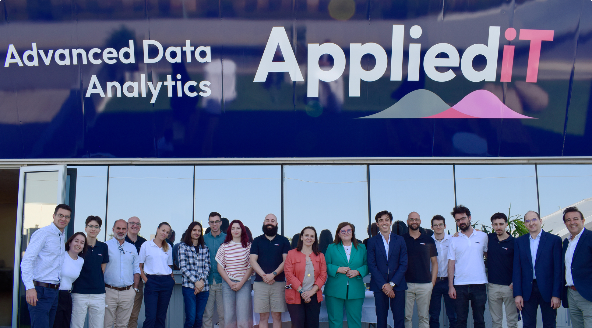
SmartMan was launched to advance automated semiconductor packaging toward zero-defect, resource-efficient manufacturing for the automotive industry.
Funded by the Federal Ministry for Economic Affairs and Energy (BMWE) and financed by the European Union, the three-year consortium brought together Bosch, Infineon Technologies, ams OSRAM, Berliner NANOTEST und Design, Chemnitzer Werkstoffmechanik (CWM), inuTech, Fraunhofer EMFT, Fraunhofer ENAS, TU Chemnitz, TU München, and AppliediT.

The objective across the value chain was to make failure-analysis methods inline-capable, detect initial defects directly in production, link process and quality data through 1:1 traceability and digital twins, and use those insights to adjust production parameters for higher zero-hour quality and long-term component reliability.
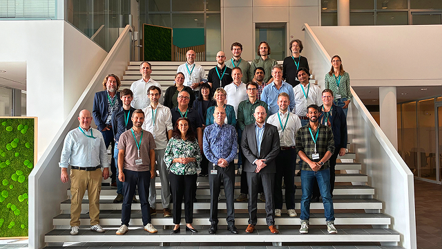
Across the consortium’s demonstrators, the partners addressed critical steps of the semiconductor production chain: bringing optical, acoustic, electrical, and thermographic inspection methods closer to the line, introducing controlled test defects, and running accelerated stress and reliability studies so that early manufacturing variations could be connected to system-level behaviour.
Within this program, AppliediT worked on the digitalization, data engineering, and analytics layer. Early in the project, it became clear that inline inspection and AI-supported diagnostics only hold up in automated production if the underlying data pipeline is stable and if candidate signals are checked against physical reality.
Tool-specific capture scripts, unversioned variable mappings, and raw measurements that mix part geometry with fixture tilt, sensor resonance, or recipe switches cannot feed automated parameter adjustments or digital twins directly.
Our approach therefore evolved into a structured workflow: standardize machine data capture, extract compact physical features from raw inspection signals, and verify through statistical and correlation studies which indicators actually reflect a defect and how they effect quality across multiple stations.
Together with the consortium partners, this resulted in concrete progress across the production chain and across multiple inspection domains:
- Optical and visual inspection analytics: In support of inline optical inspection and preassembly geometry checks, we developed automated post-processing and clustering methods for 3D height and placement scans that separate chip surfaces from side walls, quantify flatness, edge inclination, step height, and relative tilt, and isolate carrier tilt and local surface anomalies from overall package geometry.
- Acoustic defect detection: For acoustic emission testing used to investigate cracking and mechanical damage, we built feature-extraction and interactive analysis software that combines high-frequency burst waveforms with synchronous load signals, separating high-energy events from background noise and distinguishing sensor resonance from the mechanical event.
- Electrical and process correlation for wire bonding and sintering: To evaluate wire-bond quality and subsurface sinter defects, we carried out correlation studies across ultrasonic process traces, deformation measurements, and shear tests, establishing recipe-aware filtering so that process responses to real defects are separated from normal recipe differences.
- Thermographic integration and 1:1 traceability: We prepared data integration concepts for lock-in thermography and defined strict context rules—linking equipment, component identity, profile version, recipe, and evaluation method—so measurements from optical, acoustic, thermal, and process sources can be combined for cross-domain root-cause analysis and digital-twin applications.
- Standardized equipment connectivity: To connect production tools without writing custom software for every machine variant, we engineered a profile-based SECS/GEM adapter that maps variables by identifier, versions schema changes, and decouples machine acknowledgement from storage so live production is never delayed.
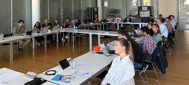
These methods and software modules now form the basis of the product we are developing at AppliediT. We are combining profile-based equipment connectivity, automated feature extraction for visual, acoustic, and process signals, and context-aware guided analytics into a modular software suite for automated manufacturing.
The SECS/GEM adapter and our evaluation applications for geometric, bond, and acoustic data have been validated on partner demonstrators, and a follow-on project with Bosch is taking the adapter toward rollout on additional equipment.
The engineering work ahead focuses on scaling these results for broader production use: calibrating optical height features across instruments against reference standards, building independently verified reference labels before deploying automated acoustic damage classifiers, completing system-wide validation of the thermography integration, and connecting the structured data outputs directly into central factory databases.
SmartMan showed that moving toward error-free semiconductor manufacturing requires both advanced inline inspection hardware and a data layer that keeps every measurement interpretable from the tool to the system level. What we carry forward into product development is that engineering discipline: configuring machine connections instead of rewriting them, reducing complex sensor signals to validated physical features, and ensuring that every data point carries the context needed for reliable automated decisions.
Share this post